

Advanced Smart PCBA Solutions Provider Enhances Next-Gen Infotainment And Instrument Cluster Assembly

Breaking Spatial Limits: Deploying Multi-Layer HDI and Microvia Technology for Complex Automotive SoCs
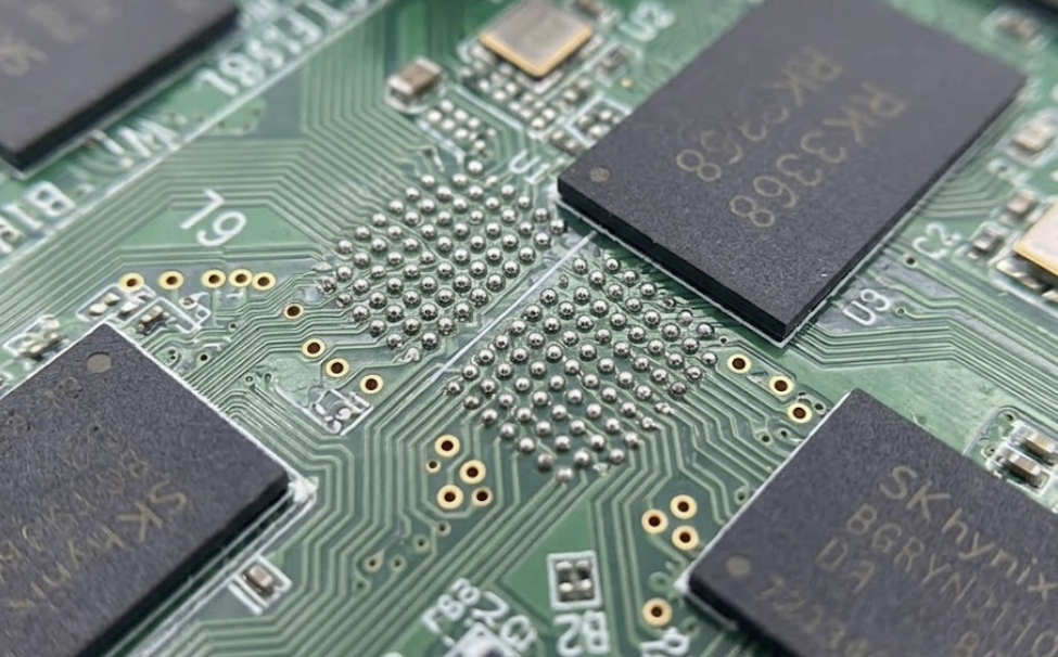
Modern cockpit domain controllers integrate multiple independent operating systems into a single, high-performance System on Chip. These advanced automotive processors feature thousands of electrical pins packed tightly into ultra-fine-pitch Ball Grid Array configurations. Consequently, standard multi-layer printed circuit board layouts can no longer accommodate the dense routing pathways necessary for these micro-components. To overcome these severe spatial boundaries, advanced manufacturing plants implement multi-layer High-Density Interconnect designs. HDI architectures deploy via-in-pad structures alongside stacked blind or buried microvias to maximize internal routing efficiency. This technical approach allows engineers to route complex high-speed signals through microscopic layers, drastically reducing the physical footprint of the motherboard. Processors with a 0.5mm pitch require laser-drilled microvias to establish clean interlayer connections without short circuits. Furthermore, technicians inspect internal layers using automated optical machines before final lamination to ensure no copper defects exist. However, sequential lamination cycles during HDI fabrication introduce significant manufacturing risks. The mismatched thermal expansion between different circuit layers can cause internal physical stress. This stress frequently leads to board warppage or micro-via fractures during subsequent heating phases. To prevent these mechanical defects, the engineering team at Aozite OST PCBA enforces strict thermal equilibrium protocols during every production cycle. Specialized automated pressing equipment applies uniform pressure and managed temperature profiles across the substrate. This rigorous methodology ensures absolute board coplanarity for subsequent high-precision surface mount assembly phases, preventing missing solder connections.
Eliminating Latency: Rigorous Signal Integrity Simulation and Strict Impedance Control for High-Frequency Circuits
High-speed automotive systems continuously transmit massive data volumes across dense, closely spaced circuit tracks. Information entertainment modules rely on rapid communication interfaces like Low-Voltage Differential Signaling and Peripheral Component Interconnect Express to render complex 3D graphics. At gigabit speeds, electrical signals behave like high-frequency radio waves rather than basic direct currents. Therefore, even minor physical variations in trace width or dielectric thickness can cause severe electromagnetic interference, signal crosstalk, or parasitic capacitance. To guarantee zero data packet loss, manufacturing experts must maintain strict characteristic impedance across every signal path. Comprehensive pre-layout and post-layout signal integrity simulations allow technicians to predict trace behavior before manufacturing begins. Engineers map copper geometries precisely to isolate high-frequency differential lines from noisy power distribution paths, using copper pours and ground fencing to block stray emissions. Interestingly, the rigorous electrical discipline required for these cabin electronics matches the high standards used in a one-stop PCBA turnkey solution for industrial control and automation equipment. Furthermore, automated optical equipment verifies track widths down to the micron level during production. By maintaining uniform solder fillet shapes and exact trace spacing, the assembly process eliminates impedance disruptions. This precision ensures real-time vehicle communication without latency, keeping safety-critical alerts functioning perfectly under all driving conditions.
Micro-Precision SMT Placement: Mastering Fine-Pitch Component Assembly and Thermally Critical Reflow Profiles
The compact environment of a modern dashboard requires the placement of ultra-small components in immediate proximity to large processing chips. Assembly lines must regularly mount miniature passive components, such as 0201 or 01005 surface-mount devices, directly adjacent to heavy BGA packages. This extreme component density leaves virtually zero margin for error during paste deposition and chip placement. Therefore, advanced factories deploy highly automated solder paste printers equipped with integrated three-dimensional inspection systems. These 3D SPI systems instantly analyze the height, area, and volume of every paste deposit to prevent short circuits or insufficient solder joints. Following paste verification, high-speed pick-and-place machinery positions components with microscopic accuracy. Afterward, the populated circuit boards enter multi-zone reflow soldering systems. Large metal shields and heavy processing chips absorb thermal energy much faster than delicate high-frequency passives. To balance these massive thermal variances, process engineers formulate highly customized reflow temperature profiles. Technicians adjust the preheat, soak, and peak reflow zones with extreme care, often utilizing vacuum reflow chambers to reduce solder void rates below ten percent. This precise thermal management ensures uniform solder melting across the entire board surface. Consequently, this step completely eliminates tombstoning defects and micro-voiding issues inside critical data connections, securing lifelong durability against harsh road conditions.
From Blueprint to High-Yield Cockpit Production: The Turnkey Solution of Aozite
Navigating multiple separate sub-vendors for circuit fabrication, component sourcing, and final assembly frequently leads to communication breakdowns and delayed timelines. In contrast, an integrated turnkey framework optimizes efficiency by combining all manufacturing stages into a single, cohesive workflow. This comprehensive approach simplifies tracking, enhances accountability, and lowers procurement costs for international automotive enterprises. Utilizing a unified engineering partner ensures that critical design adjustments propagate immediately across every production phase.
Operating from the core electronic manufacturing hub of Southern China, Aozite OST PCBA (Shenzhen Aozite Technology Co., Limited) provides the scalable infrastructure required to bring sophisticated smart products to global markets. The production facility manages eight fully automated, high-speed SMT assembly lines capable of processing over 1.2 million solder points every day. This substantial capacity ensures a seamless transition from initial engineering prototypes to high-volume commercial production. Before mass assembly begins, dedicated engineers perform exhaustive Design for Manufacturability reviews to catch potential production bottlenecks early. Furthermore, robust component verification systems protect assembly lines from counterfeit components or degraded materials. By utilizing these strict manufacturing protocols, Shenzhen Aozite Technology Co.,Limited transforms complex digital concepts into high-yield, road-ready hardware that powers the next generation of intelligent vehicle systems worldwide.
For more information regarding advanced automotive manufacturing capabilities and technical services, please visit the official corporate portal: https://www.aozite-pcba.com/.
Aozite OST PCBA
Aozite OST PCBA
Legal Disclaimer:
EIN Presswire provides this news content "as is" without warranty of any kind. We do not accept any responsibility or liability for the accuracy, content, images, videos, licenses, completeness, legality, or reliability of the information contained in this article. If you have any complaints or copyright issues related to this article, kindly contact the author above.
